
|
|
|
||||||||
|
Register or Login: | Password: |
|
|
|
|||||
|
|
|
||||||||
|
|
|
||||||||
|
|
|
|
|||||||||||||||||||||||||||||||||||||
        |  |
 | ||||||||||||||
 |
 |
 |
1 of 1 |  |
 |
 |
|
 |
|||
|
|||||
|
|
This Document | |
||
|
|
|
|||
|
|||||
|
|
 |
SummaryPlus | |
|
|
|
 |
Full Text + Links | |
|
|
|
·Thumbnail Images | |
|
|
|
|
|
PDF (308 K) | |
|
|
|
|
|||
|
|||||
|
|
|
|||
|
|
Actions | |
||
|
|
|
|||
|
|||||
|
|
|
Cited By | |
|
|
|
|
Save as Citation Alert | |
|
|
|
|
E-mail Article | |
|
|
|
|
Export Citation | |
|
 |
|
 |
|||
|
|||||

Calculation of surface optical properties: from qualitative understanding to quantitative predictions
W. G. Schmidt ,
,  , a, K. Seinoa, P. H. Hahna, F. Bechstedta, W. Lub, S. Wangb and J. Bernholc
 b
b
a Institut für Festkörpertheorie und Theoretische
Optik, Friedrich-Schiller-Universität Jena, Max-Wien-Platz 1, 07743, Jena,
Germany
b Department of Physics, North Carolina State University, Raleigh, NC 27695-8202, USA
Available online 6 February 2004.
In the last couple of years there has been much methodological and computational progress in the modeling of optical properties from first principles. While the calculation of non-linear optical coefficients is still hampered by numerical limitations—demonstrated here for the case of bulk GaAs—linear optical spectra can now be calculated accurately and with true predictive power, even for large and complex surface structures. This allows on one hand for a much better understanding of the origin of specific features such as surface optical anisotropies. We find that in particular microscopic electric fields at the surface induce slight deformations of bulk-like wavefunctions and thus give rise to optical anisotropies even from sub-surface layers. On the other hand, from the comparison of measured and calculated spectra, one can now confidently reach conclusions on the surface geometry. This short review focuses on the simulation of reflectance anisotropy spectroscopy. The clean, hydrogenated and uracil-covered Si(001) surface is used to illustrate the microscopic origin of surface optical anisotropies and the present state-of-the-art in computational modeling of optical spectra.
Author Keywords: Reflectance anisotropy spectroscopy; Density-functional calculations; Semiconductor surfaces; Second harmonic generation
78.68.+m; 78.66.Fd; 78.66.Db; 78.66.Qn
Optical spectroscopies are extremely valuable for the in situ, non-destructive and real-time surface monitoring under challenging conditions as may be encountered, e.g. during epitaxial growth. Reflectance anisotropy spectroscopy (RAS) is one of the plethora of surface sensitive spectroscopies probing linear optical coefficients, which has been particularly successful in exploring surface structures.
Already in 1966 Cardona, Pollak and Shaklee observed that rotating a Si(110) sample around the surface normal changed the reflectivity as a function of the azimuthal angle [1]. However, it took about twenty years before the phenomenon of surface-induced optical anisotropies started to be investigated systematically [2, 3, 4 and 5]. The high potential of RAS for growth-monitoring was demonstrated by Kamiya et al. [6] by measurements on GaAs(001) in ultra-high vacuum as well as in atmospheric pressure of H2, He and N2. It was noted that each of the well-known GaAs(001) surface reconstructions such as (4×4), (2×4) and (4×2) gives rise to a characteristic, fingerprint-like RAS spectrum. The correlation between reflection high-energy electron diffraction (RHEED) patterns and the RAS spectra allowed them to establish a database for GaAs(001) surface reconstructions [7]. The surface reconstruction can thus be determined in situ, even at ambient conditions. For many semiconductors a change of the surface reconstruction during layer growth occurs. RAS can, therefore be easily used to monitor growth and layer completion. This application has proven highly successful [8 and 9] and is now exploited commercially.
However, surface optical spectroscopies give only indirect information about the surface structure and chemistry. The intuitive interpretation of the spectra in terms of bond polarizabilities is difficult and often leads to wrong results even for relatively simple surfaces such as Si(001) (see discussion in Ref. [10]). Reliable calculations of surface optical spectra are needed to fully exploit their diagnostic potential.
One of the first major attempts to calculate surface optical properties was made in 1971 by McIntyre and Aspnes [11]. They approximated the inhomogeneity of the surface dielectric tensor by a two-step function, i.e. modeled the surface by a three-layer system consisting of vacuum, thin film and substrate. This model was later extended to include surface anisotropy [12] and remains very popular because of its simplicity.
A more general approach was taken in 1979 by Bagchi, Barrera and Rajagopal [13]. They started by considering a semi-infinite electron gas. The truncation of the bulk leads to a modification of the optical properties in the surface region. Based on the assumption that this region is much thinner than the light wavelength, the light propagation equations were solved. A few years later Del Sole [14] generalized this method to the case of larger anisotropies in real crystals and obtained an expression for the surface contribution to the reflectance, ΔR/R, where R is the reflectance according to the Fresnel equation. For s-light polarized along i and normal incidence one obtains
 b is the bulk dielectric function, and
Here  is the non-local macroscopic dielectric tensor of the solid-vacuum interface accounting for all many-body and local-field (LF) effects [15]. The second term in Eq. (2) is difficult to calculate because of the inversion required to obtain zz−1 and because of the four-fold integration. It contains off-diagonal terms iz of the susceptibility of the semi-infinite crystal. Manghi et al. [16]
investigated the influence of these terms for GaAs(110) and GaP(110) surfaces.
No relevant contributions of the off-diagonal terms to the reflectance were
noticed and they are therefore, usually neglected. The first term of Eq. (2)
can be evaluated by replacing the semi-infinite crystal by an artificial
super-cell, large enough to represent the vacuum as well as the surface and
bulk regions of the crystal under investigation. Provided that: (i) the slab
is large enough to properly describe the surface region of the crystal, i.e.
the surface as well as surface-modified bulk wavefunctions and (ii) the off-diagonal
terms of the dielectric tensor are small compared to the diagonal ones, a
simple expression for the surface contribution to the reflectivity can be
derived [16]
is the non-local macroscopic dielectric tensor of the solid-vacuum interface accounting for all many-body and local-field (LF) effects [15]. The second term in Eq. (2) is difficult to calculate because of the inversion required to obtain zz−1 and because of the four-fold integration. It contains off-diagonal terms iz of the susceptibility of the semi-infinite crystal. Manghi et al. [16]
investigated the influence of these terms for GaAs(110) and GaP(110) surfaces.
No relevant contributions of the off-diagonal terms to the reflectance were
noticed and they are therefore, usually neglected. The first term of Eq. (2)
can be evaluated by replacing the semi-infinite crystal by an artificial
super-cell, large enough to represent the vacuum as well as the surface and
bulk regions of the crystal under investigation. Provided that: (i) the slab
is large enough to properly describe the surface region of the crystal, i.e.
the surface as well as surface-modified bulk wavefunctions and (ii) the off-diagonal
terms of the dielectric tensor are small compared to the diagonal ones, a
simple expression for the surface contribution to the reflectivity can be
derived [16]
Here  with i=x,y
is the diagonal tensor component of the averaged half-slab polarizability.
It is important to note that under the conditions mentioned above, Eq. (3) contains in principle all
surface contributions to the optical reflectance. This includes contributions
due to surface electronic states, atomic relaxations, the influence of the
surface potential on the bulk wavefunctions as well as the surface LF effects,
i.e. the influence of the surface-modified microscopic fluctuations of the
electric field on the macroscopic dielectric response, and many-particle
effects such as the electronic self-energy and the electron–hole attraction.
Of course, it is not an easy task to include all these contributions in practical
calculations of the slab polarizability
with i=x,y
is the diagonal tensor component of the averaged half-slab polarizability.
It is important to note that under the conditions mentioned above, Eq. (3) contains in principle all
surface contributions to the optical reflectance. This includes contributions
due to surface electronic states, atomic relaxations, the influence of the
surface potential on the bulk wavefunctions as well as the surface LF effects,
i.e. the influence of the surface-modified microscopic fluctuations of the
electric field on the macroscopic dielectric response, and many-particle
effects such as the electronic self-energy and the electron–hole attraction.
Of course, it is not an easy task to include all these contributions in practical
calculations of the slab polarizability  . Up to very recently, many approximations were required to calculate .
One possibility consists in combining the atomic structure optimization within
density-functional theory (DFT) with electronic structure calculations done
in the tight-binding (TB) approximation. This method has for example been
applied to clean [17] and Sb-covered GaAs(001) surfaces [18] as well as the As/InP(110) interface [19]. Other encouraging results were obtained by combining DFT calculations with the scissors-operator approximation [20] to the electronic self-energy. This method has been applied to, among others, bare and As-terminated Si(001) surfaces [21 and 22]. Pulci et al. [23]
used a linear parametrization of the quasiparticle shifts calculated within
the GW approximation with respect to surface localization to calculate the
RAS for the GaAs cleavage face.
. Up to very recently, many approximations were required to calculate .
One possibility consists in combining the atomic structure optimization within
density-functional theory (DFT) with electronic structure calculations done
in the tight-binding (TB) approximation. This method has for example been
applied to clean [17] and Sb-covered GaAs(001) surfaces [18] as well as the As/InP(110) interface [19]. Other encouraging results were obtained by combining DFT calculations with the scissors-operator approximation [20] to the electronic self-energy. This method has been applied to, among others, bare and As-terminated Si(001) surfaces [21 and 22]. Pulci et al. [23]
used a linear parametrization of the quasiparticle shifts calculated within
the GW approximation with respect to surface localization to calculate the
RAS for the GaAs cleavage face.
While the examples discussed above allow for a meaningful interpretation of the experimental spectra, the quantitative agreement is often unsatisfactory. This has caused a considerable amount of confusion and speculation about the origin of surface optical anisotropies in the literature. Even the validity of the slab approach for the calculation of surface optical spectra was questioned. In particular the fact that surface optical spectra often show resonances near the energies of bulk critical point (CP) energies has been considered puzzling. It has led to the development of a series of models which—by choosing suitably fitted parameters—were often successful in reproducing specific features of the measured spectra:
The surface termination effect has already been shown by Del Sole and Onida [38] to be irrelevant for RAS. However, a comprehensive, quantitative picture on how strongly the surface optical anisotropies are related to surface electric fields, surface induced strain, surface defects, local fields and many-body effects such as self-energy and electron–hole attraction effects could only be obtained very recently, thanks to the advent of supercomputing and advanced numerical algorithms.
The optical anisotropy of the Si(001) surface has been intensively studied by both experiment [22, 28, 30, 40, 41, 42, 43 and 44] and theory [10, 21, 22, 45, 46 and 47], due to its technological importance and its model character for semiconductor surface science. In order to determine the origin of the spectral features of the Si(001)c(2×4) surface, Schmidt et al. [39] performed ab initio calculations based on a massively parallel real-space finite-difference implementation [48] of the DFT. Self-energy effects were taken into account using the scissors operator. A linear cut-off function was used to separate the contributions to the RAS from electronic transitions within the uppermost four atomic layers and from the bulk-like layers underneath. Fig. 1 shows that surface-state related transitions are mainly responsible for the optical anisotropies below the E1 CP energy. This holds in particular for the features T1 and T2. The appearance of optical anisotropies due to transitions between surface states is not surprising: In a number of instances such as InP, GaP and SiC surfaces, numerical modeling succeeded in relating characteristic anisotropy peaks to specific surface states [49, 50, 51, 52 and 53].
Fig. 1. RAS
for Si(001)c(2×4), calculated for the fully relaxed configuration (solid lines), a geometry where the relaxation was restricted to the uppermost two atomic layers (dashed lines) and an anisotropically strained slab (dotted lines). Shown are contributions to the RAS from electronic transitions within the uppermost four atomic layers, from the layers underneath, and the total signal. From Ref. [39]
More difficult to understand is the appearance of optical anisotropies such as T3, which are not related to transitions between surface states. It has led to the suggestion that subsurface stress due to the dimerization of the surface atoms may be largely responsible for RAS contributions from deeper layers [36]. In order to test this hypothesis additional calculations were performed for a geometry, where only the uppermost two atomic layers were allowed to relax, and the remaining atoms occupy their ideal bulk positions. Fig. 1 shows the RAS spectrum of the configuration with surface-restricted relaxation (dashed lines) in comparison with the results for the fully relaxed geometry (solid lines). The surface-related RAS minima T1 and T2 become more pronounced. Only small modifications occur for the RAS arising from electronic transitions below the uppermost four atomic layers.
A second possibility to probe the influence of surface stress on the optical spectra consists in slightly changing the lateral dimensions of the surface unit cell. The dimerized surface is stretched along the dimer bonds and compressed across the dimer rows [54]. Accordingly, the Si(001)c(2×4) surface was relaxed in a unit cell whose lateral dimensions are shrunk/enlarged by 0.5% along [110]/[110]. The RAS spectra calculated for this configuration are shown by dotted lines in Fig. 1. The optical anisotropies arising from subsurface transitions are slightly affected. In particular the T3 feature is enhanced. It may thus be partially attributed to reconstruction-induced stress in the layers beneath the surface. The calculations thus show that both the structural relaxation in the bulk and anisotropic strain fields modify the bulk-related optical anisotropy. Its salient features, however, are not affected. This indicates that the surface induces optical anisotropies in the bulk predominantly via an electronic coupling.
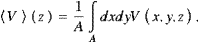
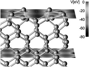
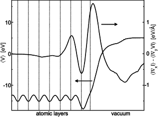
In Fig. 2 the local part of the effective potential entering the DFT Kohn–Sham equations
 in the uppermost two atomic layers differs strongly from the value in the
deeper layers. In order to quantify the anisotropy of the potential we consider
the layer-averaged microscopic electric fields perpendicular to the surface
normal. In detail, we calculate
in the uppermost two atomic layers differs strongly from the value in the
deeper layers. In order to quantify the anisotropy of the potential we consider
the layer-averaged microscopic electric fields perpendicular to the surface
normal. In detail, we calculateFig. 2. Local part of the effective potential calculated for Si(001)c(2×4) shown in two planes perpendicular to the surface normal.
Fig. 3. Averaged effective potential and its anisotropy for Si(001)c(2×4) shown along the surface normal. Dashed lines indicate the positions of the atomic layers.
Superimposed on the surface-induced anisotropies of the electron wavefunctions may be deformations due to electric fields induced by, e.g. the pinning of the Fermi level at the sample surface. These deformations may be anisotropic too, as has been shown by first-principles calculations for GaAs(001) surfaces (cf. Fig. 6 in Ref. [55]). The linear electro-optic effect modifies mainly the optical anisotropy from the bulk atomic layers, resulting in changes of the RAS signal, which are strongly reconstruction dependent, however. The electric field affects the atomic lattice as well as the electron wavefunctions and their eigenvalues. It has been found, however, that the changes of the combined density of states due to the electric field as well as the field-induced lattice relaxations are negligible compared to the deformations of the wavefunctions, resulting in modified transition matrix elements [55].
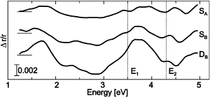
The surface potential may not only be altered by electric fields, but also by surface defects such as steps. The modified potential may on one hand lead to defect-localized electronic states, which are directly involved in electronic transitions, thus modifying the surface optical response. On the other hand, additional optical signals can be expected from perturbed bulk-like wavefunctions localized far beneath the uppermost substrate layers. Defect-induced optical anisotropies may be of similar magnitude as the signals from the perfectly ordered surface. This is demonstrated in Fig. 4, where we have plotted the calculated optical anisotropies due to the three most commonly observed step configurations on Si(001) surfaces [56]: SA steps and rebonded steps of type SB and DB [39]. The calculated step-related anisotropies (which are in excellent agreement with experiment [41]) explain the distinct differences in the RAS spectra measured for different Si(001) surface samples [22, 40, 41 and 42].
Fig. 4. Step-induced optical anisotropy
The inclusion of many-body effects—beyond those already contained in the approximations for exchange and correlation, which enter the Kohn–Sham equations—in the calculation of surface optical spectra is a fairly recent achievement. In the late 1990s it has become possible to correct the single-particle excitation energies for quasiparticle effects, using approximations to the self-energy within the GW approach [23, 49 and 57]. The solution of the Bethe–Salpeter equation (BSE) allows electron–hole attraction, i.e. excitonic, and LF contributions to the surface optical response to be taken into account. While the first applications of the BSE to surfaces were restricted to the description of few strongly localized surface states [58 and 59], advanced algorithms together with a massive parallelization of the computations made it recently possible to model the excitonic and LF effects in a wide spectral range [60 and 61].
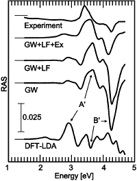
In Fig. 5 the influence of many-body effects on the calculated optical anisotropy of the monohydride Si(001)(2×1) surface [61]
is shown. The spectrum calculated in the independent-particle approximation,
i.e. the DFT-LDA spectrum shows in principle the features observed experimentally
[43]. However, the calculated A′ and B′ peaks are redshifted
in comparison with the experiment by 0.5 eV and 0.8 eV, respectively. Self-energy
corrections calculated in GW approximation shift the excitation energies
to larger values. Furthermore, the B′ optical anisotropy is much increased.
This is not only related to the non-uniform self-energy corrections of the
DFT-LDA eigenvalues, but also a consequence of the  scaling of the surface contribution to the reflectance (cf. Eq. (1)).
Surface LF effects can be expected from both the microscopic fluctuations
of the electric field within the bulk, and from the truncation of the bulk
itself. The numerical calculation, however, shows that LF effects lead to
surprisingly small changes of the spectrum in the particular case studied
here. A distinct change of the RAS spectrum, however, results from the inclusion
of the attractive electron–hole interaction. A strong reduction of the B′
optical anisotropy and an increase of the integrated A′ peak area occurs.
At the same time, the A′ and B′ optical anisotropies are shifted to lower
energies by approximately 0.2 eV.
scaling of the surface contribution to the reflectance (cf. Eq. (1)).
Surface LF effects can be expected from both the microscopic fluctuations
of the electric field within the bulk, and from the truncation of the bulk
itself. The numerical calculation, however, shows that LF effects lead to
surprisingly small changes of the spectrum in the particular case studied
here. A distinct change of the RAS spectrum, however, results from the inclusion
of the attractive electron–hole interaction. A strong reduction of the B′
optical anisotropy and an increase of the integrated A′ peak area occurs.
At the same time, the A′ and B′ optical anisotropies are shifted to lower
energies by approximately 0.2 eV.
Fig. 5. RAS spectra
The stepwise inclusion of many-particle effects in the calculation leads to a considerable and systematic improvement of the agreement with the experiment. The remaining discrepancies are mainly due to the numerical limitations of the study [61], in particular with respect to the slab thickness and Brillouin zone sampling.
The full inclusion of many-body effects in the calculation of surface optical spectra leads to the limits of today's computer capacity. However, numerically well-converged spectra calculated within the independent-particle approximation and using the scissors-operator approach to account for the band-gap underestimation are in many instances sufficient for the reliable prediction of surface optical anisotropies. This is because RAS spectra are difference spectra, which are furthermore normalized to the bulk dielectric function (cf. Eq. (1)). Many systems, for example surface defects or very large reconstructions such as the ones formed by In nanowires on Si(111) surfaces [62] can presently only be described within the single-particle approximation.
Organic functionalization of semiconductors has become important for the development of new semiconductor-based devices. The physical and chemical properties of hybrid organic/inorganic materials depend crucially on the structural and chemical details of the interface. In principle it should be possible to obtain such information from optical spectroscopies such as RAS. However, at present there are only relatively few experimental and theoretical studies that explore optical anisotropies of organically modified semiconductors (see, e.g. Refs. [63, 64 and 65]).
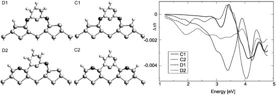
The adsorption of uracil on Si(001), investigated experimentally by scanning tunneling microscopy and high-resolution electron energy-loss spectroscopy [66], leads to what can be considered a prototypical interface between a polyfunctional molecule and a semiconductor surface. The (001) surface of silicon is the starting point for the fabrication of most microelectronic devices. Uracil (C4H4N2O2) is a small molecule featuring one C=C double bond, two amino and two carbonyl groups and may thus bond to the surface in various ways. In addition, its tautomerism and electrostatic effects have been found to be important for the interface formation [66 and 67]. In order to probe the sensitivity of RAS with respect to different uracil bonding configurations we calculate spectra for the most relevant dative (D1, D2 in Fig. 6) and covalently bonded (C1, C2) interface configurations (details will be published elsewhere). These spectra (Fig. 6) indicate that the adsorption of organic molecules strongly modifies the optical response of the Si(001) surface (cf. Fig. 1) and leads to a signal that is very sensitive to the details of the interface. In particular for photon energies of approximately 3.3 eV, i.e. slightly below the E1 CP, a strong dependence of the surface optical anisotropy on the adsorption configuration can be stated: oxygen insertion into the uppermost Si dimers (D2, C2) leads to a strong negative anisotropy. However, also the structures where uracil remains intact, and is dative (D1) or covalently bonded to the substrate (C1) can be clearly distinguished by means of RAS.
Fig. 6. Left: Uracil/Si(001) adsorption configurations. White, gray, dark gray, dark, and small symbols indicate C, N, Si, O, and H atoms, respectively. Right: RAS
RAS spectra simulated for cyclopentene adsorption configurations on Si(001) [65] indicate that measurements of reflectance difference data can even discriminate between ‘cis’ and ‘trans-type’ adsorption configurations. The high sensitivity of RAS with respect to the details of the surface chemical bonding in conjunction with the accuracy achieved in the numerical prediction of such spectra thus suggests RAS as a powerful tool also for monitoring the formation of organic thin films.
Thus
far we have focused on the modeling of linear optical spectra. However, non-linear
optical processes such as second harmonic generation (SHG) are also increasingly
being used for surface and interface analysis [71].
Unfortunately, the microscopic interpretation of the measured spectra is
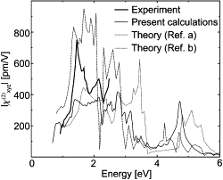
severely hampered by numerical difficulties. This is demonstrated in Fig. 7, where we compare recently calculated values for the second-harmonic susceptibility  of bulk GaAs with experiment [68]. Obviously, the theoretical results obtained within a full-potential linearized augmented plane-wave method [70] and from plane-wave pseudopotential calculations [69] neither agree well with each other nor with the present calculations utilizing a real-space finite-difference approach [48].
The agreement between theory and experiment is also unsatisfactory. The reasons
for the discrepancies are on the one hand related to the extreme sensitivity
of the calculations to nearly all technical parameters, in particular the
sampling of the Brillouin zone (in the present calculations a set of 32 000
randomly chosen points was needed to obtain converged results). On the other
hand, non-linear optical spectra depend on many-body effects in a complex
and not easily predictable manner [69 and 72]
(in the present calculations a scissors-operator approach was used). Both,
the technical aspects as well as the correct modeling of many-body effects
become much more difficult to control in the case of surface calculations
[73], where it seems presently
that only empirical models using fitted values for the bond polarizabilities
allow for the satisfactory modeling of surface SHG spectra [74].
Thus, for non-trivial cases neither a qualitative understanding nor a quantitative
prediction of non-linear surface optical spectra seems presently possible.
of bulk GaAs with experiment [68]. Obviously, the theoretical results obtained within a full-potential linearized augmented plane-wave method [70] and from plane-wave pseudopotential calculations [69] neither agree well with each other nor with the present calculations utilizing a real-space finite-difference approach [48].
The agreement between theory and experiment is also unsatisfactory. The reasons
for the discrepancies are on the one hand related to the extreme sensitivity
of the calculations to nearly all technical parameters, in particular the
sampling of the Brillouin zone (in the present calculations a set of 32 000
randomly chosen points was needed to obtain converged results). On the other
hand, non-linear optical spectra depend on many-body effects in a complex
and not easily predictable manner [69 and 72]
(in the present calculations a scissors-operator approach was used). Both,
the technical aspects as well as the correct modeling of many-body effects
become much more difficult to control in the case of surface calculations
[73], where it seems presently
that only empirical models using fitted values for the bond polarizabilities
allow for the satisfactory modeling of surface SHG spectra [74].
Thus, for non-trivial cases neither a qualitative understanding nor a quantitative
prediction of non-linear surface optical spectra seems presently possible.
Fig. 7. Spectral dependence of
of GaAs as measured [68] and calculated here and in Refs. [69] (a) and [70] (b), respectively.
The difference between the optical
response of the surface compared to that of the bulk may be related to the
possible presence of surface electronic states, but can also arise from surface
induced anisotropies in the crystal potential extending far below the uppermost
surface layer, surface electric fields, surface defects, and surface induced
strain fields. It has now become possible to include these effects highly
accurately in parameter-free calculations of linear surface optical spectra.
Even many-body effects such as self-energy and excitonic contributions to
the optical response and the influence of local fields can now be studied
from first principles. Quantitative predictions of linear surface
optical properties have thus become possible. The accuracy of calculated
non-linear optical properties, however, still suffers from numerical limitations.
Grants of computer time from
the DoD Challenge Program, the Leibniz-Rechenzentrum München, and the Höchstleistungsrechenzentrum
Stuttgart are gratefully acknowledged.
1. M. Cardona, F.H. Pollak and K.L. Shaklee. J. Phys. Soc. Jpn. 21 Suppl. (1966), p. 89.
2. P. Chiaradia, A. Cricenti, S. Selci and G. Chiarotti. Phys. Rev. Lett. 52 (1984), p. 1145. Abstract-INSPEC | Full Text via CrossRef
3. M.A. Olmstead and N.M. Amer. Phys. Rev. Lett. 52 (1984), p. 1148. Abstract-INSPEC | Full Text via CrossRef
4. D.E. Aspnes and A.A. Studna. Phys. Rev. Lett. 54 (1985), p. 1956. Abstract-INSPEC | Full Text via CrossRef
5. V.L. Berkovits, I.V. Makarenko, T.A. Minashvili and V.I. Safarov. Solid State Commun. 56 (1985), p. 449. Abstract | Abstract + References | PDF (211 K)
6. I. Kamiya, D.E. Aspnes, H. Tanaka, L.T. Florez, J.P. Harbison and R. Bhat. Phys. Rev. Lett. 68 (1992), p. 627. Abstract-INSPEC | Full Text via CrossRef
7. I. Kamiya, D.E. Aspnes, L.T. Florez and J.P. Harbison. Phys. Rev. B 46 (1992), p. 15894. Abstract-INSPEC | Full Text via CrossRef
8. N. Dietz, U. Rossow, D.E. Aspnes and K.J. Bachmann. J. Electr. Mat. 24 (1995), p. 1571. Abstract-INSPEC
9. J. Zettler, K. Haberland, M. Zorn, M. Pristovsek, W. Richter, P. Kurpas and M. Weyers. J. Cryst. Growth 195 (1998), p. 151. SummaryPlus | Full Text + Links | PDF (494 K)
10. C. Kress, A.I. Shkrebtii and R. Del Sole. Surf. Sci. 377 (1997), p. 398. SummaryPlus | Full Text + Links | PDF (593 K)
11. J.D.E. McIntyre and D.E. Aspnes. Surf. Sci. 24 (1971), p. 417. Abstract | Abstract + References | PDF (926 K)
12. K. Hingerl, D.E. Aspnes, I. Kamiya and L.T. Florez. Appl. Phys. Lett. 63 (1993), p. 885. Abstract-INSPEC | Full Text via CrossRef
13. A. Bagchi, R.G. Barrera and A.K. Rajagopal. Phys. Rev. B 20 (1979), p. 4824. Abstract-INSPEC | Full Text via CrossRef
14. R. Del Sole. Solid State Commun. 37 (1981), p. 537. Abstract | Abstract + References | PDF (353 K)
15. R. Del Sole and E. Fiorino. Phys. Rev. B 29 (1984), p. 4631. Abstract-INSPEC | Full Text via CrossRef
16. F. Manghi, R. Del Sole, A. Selloni and E. Molinari. Phys. Rev. B 41 (1990), p. 9935. Abstract-INSPEC | Full Text via CrossRef
17. A.I. Shkrebtii, N. Esser, W. Richter, W.G. Schmidt, F. Bechstedt, B.O. Fimland, A. Kley and R. Del Sole. Phys. Rev. Lett. 81 (1998), p. 721. Abstract-INSPEC | APS full text | Full Text via CrossRef
18. N. Esser, A.I. Shkrebtii, U. Resch-Esser, C. Springer, W. Richter, W.G. Schmidt, F. Bechstedt and R.D. Sole. Phys. Rev. Lett. 77 (1996), p. 4402. APS full text | Full Text via CrossRef
19. P.V. Santos, B. Koopmans, N. Esser, W.G. Schmidt and F. Bechstedt. Phys. Rev. Lett. 77 (1996), p. 759. Abstract-INSPEC | APS full text | Full Text via CrossRef
20. R. Del Sole and R. Girlanda. Phys. Rev. B 48 (1993), p. 11789. Abstract-INSPEC | Full Text via CrossRef
21. M. Palummo, G. Onida, R. Del Sole and B.S. Mendoza. Phys. Rev. B 60 (1999), p. 2522. Abstract-INSPEC | APS full text | Full Text via CrossRef
22. L. Kipp, D.K. Biegelsen, J.E. Northrup, L.-E. Swartz and R.D. Bringans. Phys. Rev. Lett. 76 (1996), p. 2810. Abstract-INSPEC | APS full text | Full Text via CrossRef
23. O. Pulci, G. Onida, R. Del Sole and L. Reining. Phys. Rev. Lett. 81 (1998), p. 5374. Abstract-INSPEC | APS full text | Full Text via CrossRef
24. C.H. Wu and W. Hanke. Solid State Commun. 23 (1977), p. 829. Abstract | Abstract + References | PDF (329 K)
25. W.L. Mochán and R.G. Barrera. Phys. Rev. Lett. 55 (1985), p. 1192. Abstract-INSPEC | Full Text via CrossRef
26. B.S. Mendoza and W.L. Mochán. Phys. Rev. B 55 (1997), p. 2489. Abstract-INSPEC | APS full text | Full Text via CrossRef
27. B.S. Mendoza, R. Del Sole and A.I. Shkrebtii. Phys. Rev. B 57 (1998), p. R12709. APS full text | Full Text via CrossRef
28. L. Mantese, U. Rossow and D.E. Aspnes. Appl. Surf. Sci. 107 (1996), p. 35. Abstract | Abstract + References | PDF (546 K)
29. L. Mantese, K.A. Bell, U. Rossow and D.E. Aspnes. J. Vac. Sci. Technol. B 15 (1997), p. 1196. Abstract-INSPEC | OJPS full text | Full Text via CrossRef
30. U. Rossow, L. Mantese and D.E. Aspnes. J. Vac. Sci. Technol. B 14 (1996), p. 3070. Abstract-INSPEC | OJPS full text | Full Text via CrossRef
31. L. Mantese, K.A. Bell, D.E. Aspnes and U. Rossow. Phys. Lett. A 253 (1999), p. 93. Abstract | Abstract + References | PDF (465 K)
32. D.E. Aspnes, L. Mantese, K.A. Bell and U. Rossow. Phys. Stat. Sol. (B) 220 (2000), p. 709. Abstract-INSPEC | Full Text via CrossRef
33. K. Uwai and N. Kobayashi. Phys. Rev. Lett. 78 (1997), p. 959. Abstract-INSPEC | APS full text | Full Text via CrossRef
34. L.F. Lastras-Martinez and A. Lastras-Martinez. Phys. Rev. B 54 (1996), p. 10726. Full Text via CrossRef
35. A. Lastras-Martinez, R.E. Balderas-Navarro, L.F. Lastras-Martinez and M.A. Vidal. Phys. Rev. B 59 (1999), p. 10234. Abstract-INSPEC | Full Text via CrossRef
36. K. Hingerl, R.E. Balderas-Navarro, W. Hilber, A. Bonanni and D. Stifter. Phys. Rev. B 62 (2000), p. 13048. Abstract-INSPEC | Full Text via CrossRef
37. K. Hingerl, R.E. Balderas-Navarro, A. Bonanni, P. Tichopadek and W.G. Schmidt. Appl. Surf. Sci. 175–176 (2001), p. 769. SummaryPlus | Full Text + Links | PDF (168 K)
38. R. Del Sole and G. Onida. Phys. Rev. B 60 (1999), p. 5523.
39. W.G. Schmidt, F. Bechstedt and J. Bernholc. Phys. Rev. B 63 (2001), p. 045322.
40. T. Yasuda, L. Mantese, U. Rossow and D.E. Aspnes. Phys. Rev. Lett. 74 (1995), p. 3431. Abstract-Compendex | Abstract-INSPEC | Full Text via CrossRef
41. S.G. Jaloviar, J.-L. Lin, F. Liu, V. Zielasek, L. McCaughan and M.G. Lagally. Phys. Rev. Lett. 82 (1999), p. 791. Abstract-INSPEC | APS full text | Full Text via CrossRef
42. R. Shioda and J. van der Weide. Phys. Rev. B 57 (1998), p. R6823. Abstract-INSPEC | APS full text | Full Text via CrossRef
43. R. Shioda and J. van der Weide. Appl. Surf. Sci. 130–132 (1998), p. 266. SummaryPlus | Full Text + Links | PDF (149 K)
44. U. Rossow, L. Mantese, D.E. Aspnes, K.A. Bell and M. Ebert. Phys. Stat. Sol. B 215 (1999), p. 725. Abstract-INSPEC | Full Text via CrossRef
45. A.I. Shkrebtii and R. Del Sole. Phys. Rev. Lett. 70 (1993), p. 2645. Abstract-INSPEC | Full Text via CrossRef
46. V.I. Gavrilenko and F.H. Pollak. Phys. Rev. B 58 (1998), p. 12964. Abstract-INSPEC | APS full text | Full Text via CrossRef
47. N. Arzate and B.S. Mendoza. Phys. Rev. B 63 (2001), p. 3303.
48. E.L. Briggs, D.J. Sullivan and J. Bernholc. Phys. Rev. B 54 (1996), p. 14362. Abstract-INSPEC | Full Text via CrossRef
49. W.G. Schmidt, N. Esser, A.M. Frisch, P. Vogt, J. Bernholc, F. Bechstedt, M. Zorn, T. Hannappel, S. Visbeck, F. Willig and W. Richter. Phys. Rev. B. 61 (2000), p. R16335. APS full text | Full Text via CrossRef
50. W.G. Schmidt, E.L. Briggs, J. Bernholc and F. Bechstedt. Phys. Rev. B 59 (1999), p. 2234. Abstract-INSPEC | APS full text | Full Text via CrossRef
51. W.G. Schmidt, J. Bernholc and F. Bechstedt. Appl. Surf. Sci. 166 (2000), p. 179. SummaryPlus | Full Text + Links | PDF (257 K)
52. P.H. Hahn, W.G. Schmidt, F. Bechstedt, O. Pulci, R. Del Sole, Phys. Rev. B (accepted)
53. W. Lu, W.G. Schmidt, E.L. Briggs and J. Bernholc. Phys. Rev. Lett. 85 (2000), p. 4381. Abstract-Compendex | Full Text via CrossRef
54. J. Dabrowski and H.-J. Müssig. Silicon Surfaces and Formation of Interfaces, World Scientific, Singapore (2000).
55. W.G. Schmidt, F. Bechstedt, W. Lu and J. Bernholc. Phys. Rev. B 66 (2002), p. 085334.
56. D.J. Chadi. Phys. Rev. Lett. 59 (1987), p. 1691. Abstract-INSPEC | Full Text via CrossRef
57. W.G. Schmidt, J.L. Fattebert, J. Bernholc and F. Bechstedt. Surf. Rev. Lett. 6 (1999), p. 1159. Abstract-INSPEC | Full Text via CrossRef
58. M. Rohlfing and S.G. Louie. Phys. Rev. Lett. 83 (1999), p. 856. Abstract-INSPEC | APS full text | Full Text via CrossRef
59. M. Rohlfing, M. Palummo, G. Onida and R. Del Sole. Phys. Rev. Lett. 85 (2000), p. 5440. Abstract-INSPEC | Abstract-Compendex | Full Text via CrossRef
60. P.H. Hahn, W.G. Schmidt and F. Bechstedt. Phys. Rev. Lett. 88 (2002), p. 016402.
61. W.G. Schmidt, S. Glutsch, P.H. Hahn and F. Bechstedt. Phys. Rev. B 67 (2003), p. 085307.
62. S. Wang, W. Lu, W.G. Schmidt and J. Bernholc. Phys. Rev. B 68 (2003), p. 035329.
63. A. Sassella, A. Borghesi, F. Meinardi, R. Tubono, M. Gurioli, C. Botta, W. Porzio and G. Barbarella. Phys. Rev. B 62 (2000), p. 11170. Abstract-INSPEC | Full Text via CrossRef
64. A.M. Paraian, U. Rossow, S. Park, G. Salvan, M. Friedrich, T.U. Kampen and D.R.T. Zahn. J. Vac. Sci. Technol. B 19 (2001), p. 1658. Abstract-INSPEC | Abstract-Compendex | Full Text via CrossRef
65. W. Lu, W.G. Schmidt and J. Bernholc. Phys. Rev. B 68 (2003), p. 115327.
66. A. Lopez, Q. Chen and N.V. Richardson. Surf. Interface Anal. 33 (2002), p. 441. Abstract-Compendex | Abstract-INSPEC | Full Text via CrossRef
67. K. Seino, W.G. Schmidt, M. Preuss and F. Bechstedt. J. Phys. Chem. B 107 (2003), p. 5031. Abstract-INSPEC | Abstract-Compendex | Full Text via CrossRef
68. S. Bergfeld and W. Daum. Phys. Rev. Lett. 90 (2003), p. 036801.
69. B. Adolph and F. Bechstedt. Phys. Rev. B 57 (1998), p. 6519. Abstract-INSPEC | APS full text | Full Text via CrossRef
70. J.L.P. Hughes and J.E. Sipe. Phys. Rev. B 53 (1996), p. 10751. Abstract-INSPEC | Full Text via CrossRef
71. M.C. Downer, B.S. Mendoza and V.I. Gavrilenko. Surf. Interface Anal. 31 (2001), p. 966. Abstract-Compendex | Abstract-INSPEC | Full Text via CrossRef
72. E.K. Chang, E.L. Shirley and Z.H. Levine. Phys. Rev. B 65 (2002), p. 035205.
73. J.E. Mejia, B.S. Mendoza, M. Palummo, G. Onida, R. Del Sole, S. Bergfeld and W. Daum. Phys. Rev. B 66 (2002), p. 195329.
74. G.D. Powell, J.-F. Wang and D.E. Aspnes. Phys. Rev. B 65 (2002), p. 205320.
|
|||||||||||||||||||||||||||||||||||||||||||||||||||||||||||||||||||||||||||||||||||||||||||||||||||||||||||||||||||||||
Volumes 455-456 , 1 May 2004, Pages 764-771 The 3rd International Conference on Spectroscopic Ellipsometry |
|||||||||||||||||||||||||||||||||||||||||||||||||||||||||||||||||||||||||||||||||||||||||||||||||||||||||||||||||||||||
|
|
| | 1 of 1 | |
|
|
|
| Copyright © 2004 Elsevier B.V. All rights reserved. ScienceDirect® is a registered trademark of Elsevier B.V. |